

Amazon’s custom silicon division, which designs the Trainium AI accelerator, Graviton server processor, and Nitro networking chips, is now running at an annualized revenue pace of roughly $20 billion, according to disclosures from CEO Andy Jassy. The unit has grown at a triple-digit percentage rate year-over-year, fueled almost entirely by demand for Trainium chips used to train and run AI models. Jassy said the business already holds more than $225 billion in multi-year revenue commitments, describing the figure as contracted demand rather than a forecast. Anthropic accounts for a major share of that backlog, with a multi-year, multi-gigawatt agreement tied to over $100 billion in AWS spending. OpenAI has separately committed to roughly two gigawatts of Trainium compute capacity. Amazon’s second-generation Trainium2 chip, which offers about 30% better price-performance than comparable GPUs, is largely sold out. Trainium3, which began shipping in early 2026, delivers a further 30-40% price-performance improvement over its predecessor and is already close to fully subscribed, according to the company. Even Trainium4, not expected for broad availability for another 18 months, has attracted significant advance reservations. Jassy noted that if Amazon’s chip unit operated as a standalone company selling silicon the way traditional chipmakers do, it could generate around $50 billion annually, placing it among the top three data center chip businesses in the world. The disclosures come as Amazon continues to position custom silicon as a way to reduce dependence on Nvidia GPUs and control costs across its AWS cloud infrastructure. Sources: The Motley Fool, The Register

TSMC Posts Record Profit, Adds $100 Billion to Arizona Investment as AI Chip Demand Surges
Taiwan Semiconductor Manufacturing Company (TSMC), the world’s largest contract chipmaker, reported record second-quarter 2026 results driven by surging demand for artificial intelligence chips, and announced an additional $100 billion investment in its Arizona manufacturing operations. The company posted second-quarter revenue of NT$1.27 trillion (approximately $40.2 billion), up 36% year-over-year. Net income reached NT$706.56 billion, a 77.4% increase from the same period last year, marking a record for the fifth consecutive quarter. High-performance computing chips, the category that includes AI accelerators, accounted for 66% of quarterly revenue, underscoring how central AI workloads have become to TSMC’s business. CEO C.C. Wei announced the new $100 billion commitment for Arizona, bringing the company’s total pledged investment in the state to $265 billion. The funding is earmarked for additional fabrication plants capable of producing chips at the 2-nanometer node and below, along with advanced packaging facilities. Reports indicate the expansion could support the construction of up to four more fabs, aimed at easing bottlenecks in AI chip packaging capacity. Looking ahead, TSMC raised its full-year 2026 revenue growth outlook to more than 40% in U.S. dollar terms, citing sustained demand from AI infrastructure buildouts by major cloud and chip design customers. The results reinforce TSMC’s position as the primary manufacturing partner for the world’s leading AI chip designers, even as geopolitical pressure continues to push the company toward diversifying production outside Taiwan. Sources: Data Center Dynamics, Tech Times
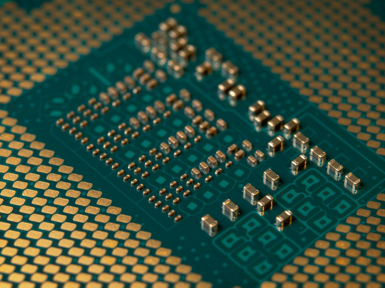
IBM unveils the first sub-1-nanometer chip and ushers in the “angstrom era.”
On June 25, 2026, IBM announced the development of the world’s first sub-nanometer chip, featuring transistors at the 0.7 nm (7-angstrom) node. This breakthrough was achieved not through the traditional method of shrinking transistor size, but via a completely new architecture called “nanostack.” How nanostack works Instead of continuing to shrink transistors on a horizontal plane—the method the industry has used for decades and which is now reaching its physical limits—IBM vertically stacks two wafers of nanosheet-type transistors, creating a “sandwich” of silicon layers. Each layer can utilize different materials, independently optimized for either performance or energy efficiency. This represents sequential 3D integration, not merely miniaturization. The numbers The result is nearly 100 billion transistors on a chip the size of a fingernail—virtually double the density of the 2 nm chip IBM unveiled in 2021. Compared to that 2 nm chip, the new node promises up to 50% higher performance, 70% greater energy efficiency, and a 40% improvement in SRAM scaling—a crucial factor for chips handling high-bandwidth AI workloads. Manufacturing location Development is taking place at IBM’s semiconductor research center in Albany, New York, which will incorporate ASML’s High-NA EUV lithography to print circuits with greater precision. Future impact IBM estimates that this architecture provides at least another decade of scaling headroom—critical at a time when Moore’s Law, as traditionally understood, was considered to have run its course. The company projects a realistic production timeline of about five years. Its most immediate applications target cloud infrastructure, generative AI, and next-generation electronic devices, areas where the demand for efficient computing is growing faster than current manufacturing capacity. “It’s not just about making transistors smaller; we are reinventing how chips are built to achieve vastly greater power and energy efficiency,” explained Jay Gambetta, Director of IBM Research. “Progress doesn’t stop; it just needs a new paradigm,” summarized Huiming Bu, IBM’s Vice President of Silicon Technology. Main source: IBM Newsroom. Also verified on TechMyMoney.